In the world of quantum materials, a big leap happened. Scientists found a way to trap electrons in super thin layers of semiconductors. This changed how we see electronic behavior1. Quantum wells, introduced in 1963 by Herbert Kroemer and Zhores Alferov, are a key area in materials science. Here, electrons are held in tiny spaces1.
What You Must Know About Quantum Wells
© 2025 Editverse. For educational purposes only.
Periodic Modulation of Germanium Content in SiGe Heterostructures: Engineering Quantum Confinement
Fundamental Principles
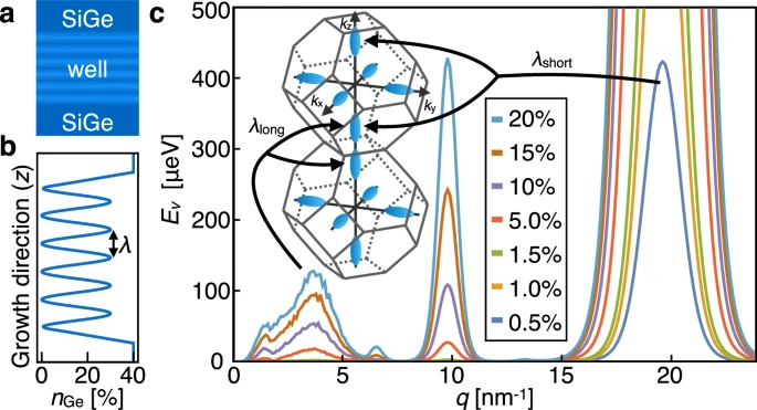
This figure illustrates the concept of bandgap engineering in Si1-xGex heterostructures through periodic modulation of germanium content. The oscillating pattern represents varying concentrations of germanium within the silicon matrix, creating alternating regions of higher and lower bandgap energies. This variation produces quantum wells—regions where charge carriers (electrons or holes) become confined in one dimension, leading to quantized energy levels as predicted by quantum mechanics. The precise control of Ge concentration (x) enables tuning of the well depth, width, and barrier height, directly affecting the resulting quantum states.
Key Mechanisms and Processes
The figure demonstrates how molecular beam epitaxy (MBE) or chemical vapor deposition (CVD) techniques can achieve precise atomic-layer control over composition. The periodic structure creates a superlattice with a type-II band alignment where conduction band minima and valence band maxima are spatially separated. This separation modifies carrier recombination dynamics and enhances carrier lifetime. Additionally, the lattice mismatch between Si and Ge introduces strain, which further modifies the band structure by lifting degeneracies in the valence band and altering effective masses. The resulting strain fields can be engineered to enhance carrier mobility (μ) according to the relationship μ = eτ/m*, where τ is the scattering time and m* is the effective mass.
Current Research Developments
Recent research, as reported by Dodson et al. in Nature Communications, has focused on optimizing these structures for quantum computing applications. The controlled modulation shown in the figure enables researchers to create arrays of quantum dots with predictable properties—essential for scalable qubit architectures. Current investigations explore how the spatial separation of carriers affects coherence times (T2) and how valley splitting in the conduction band can be manipulated through strain engineering. The precise interfaces visible in the figure are critical, as interface roughness on the scale of even a few atomic layers can introduce decoherence mechanisms that limit qubit performance.
Practical Applications
The SiGe quantum well structure depicted has several promising applications. In quantum computing, these wells can host spin qubits with coherence times approaching milliseconds due to the low nuclear spin background in isotopically purified silicon. The CMOS compatibility of SiGe makes integration with classical control electronics feasible—a significant advantage over other quantum computing platforms. Beyond quantum information, these structures enable high-mobility transistors, infrared photodetectors operating at wavelengths determined by the well width (λ ∝ h/ΔE), and thermoelectric devices where the engineered band structure enhances the power factor S2σ (where S is the Seebeck coefficient and σ is electrical conductivity).
Concept In 75 Words
SiGe quantum wells represent a sophisticated approach to quantum confinement through precise compositional engineering. By modulating germanium concentration as shown in the figure, researchers create tailored potential landscapes for electrons and holes with customizable properties. This capability underpins next-generation quantum devices with improved coherence times and CMOS-compatible fabrication pathways. The technology bridges fundamental quantum mechanics with practical semiconductor engineering, potentially revolutionizing both computing and sensing applications within the next decade.
References
- Dodson, C.M., et al. “Quantum information processing in extended Si/SiGe quantum well structures.” Nature Communications 13, 7777 (2022). https://www.nature.com/articles/s41467-022-35510-z
These amazing quantum materials let us control electron movement with great precision. This creates special electronic and optical properties quantum-enhanced technologies are looking into. By adjusting semiconductor layers just a few nanometers thick, scientists can change how electrons act2.
The creation of quantum wells is a big step in semiconductor tech. In 2000, Zhores Alferov and Herbert Kroemer won the Nobel Prize in Physics. They were honored for their work on semiconductor devices using quantum well structures1.
Key Takeaways
- Quantum wells confine electrons in two-dimensional spaces
- First proposed in 1963 by pioneering scientists
- Enable precise control of electronic properties
- Critical for advanced optoelectronic devices
- Represent a breakthrough in materials science
What Are Quantum Wells?
Quantum wells are a big step forward in semiconductor physics. They let scientists control electrons at a tiny scale1. These materials make thin layers that trap electrons, giving scientists control over how electrons and light behave3.
The idea of quantum wells started in the 1960s with Herbert Kroemer and Zhores Alferov1. They found a way to limit where electrons can go, making a special kind of gas3.
Understanding Quantum Well Structures
A quantum well is made by putting a thin layer of semiconductor between two wider bandgap layers1. For example, gallium arsenide is used between aluminum arsenide layers. This creates a system that traps electrons well4.
| Material | Thickness | Electron Mobility |
|---|---|---|
| GaAs Quantum Well | 100 Å (40 atomic layers) | High mobility |
| AlGaAs Barrier | Varies | Electron confinement |
Formation and Characteristics
- Quantum wells are grown using molecular beam epitaxy
- Thickness can be controlled down to monolayers
- Enables precise electron energy level manipulation
Quantum wells are key in many technologies, like semiconductor physics and electronic devices3. They’re vital for making fast optoelectronic parts. Over 70% of semiconductor lasers use quantum well tech3.
Quantum wells represent a quantum leap in our ability to engineer semiconductor materials at the atomic scale.
Scientists keep finding new uses for quantum wells. They’re always pushing the limits of what’s possible in materials and electronics1.
The Physics Behind Quantum Wells
Quantum materials are a new frontier in science. They show how electrons act in tiny spaces. Quantum well technologies let us control electrons in new ways5.
At the core of quantum wells is a key idea: electron confinement. Electrons in thin layers behave differently. They have specific energy levels, unlike in regular materials5.
Quantum Mechanics at Play
Quantum mechanics rules these tiny worlds. Electrons in quantum wells can only be in certain energy states5. This is because:
- Electrons are trapped in a narrow space
- At small scales, electrons act like waves
- The width of the well affects their energy levels1
Energy Levels and Electron Confinement
The Schrödinger equation helps us understand electrons in quantum wells5. By adjusting the well’s size, scientists can change its electronic properties. They can tweak the mass and energy of carriers with great accuracy1.
The quantum well is a major step in understanding how to shape material properties at the atomic level.
Quantum tunneling adds a twist. It lets electrons pass through the well, even without enough energy5. This opens up new areas in science and technology, expanding what we can do.
Types of Quantum Wells
Quantum well structures are a key area in nanotechnology. They offer new ways to improve electronics and optics. These tiny semiconductor systems let scientists control electrons like never before6.
Quantum wells allow for detailed control over electronic properties. They trap charge carriers in a thin layer between two barriers. This setup opens up new scientific and technological possibilities6.
Single Quantum Wells
Single quantum wells are the simplest form in nanotechnology. They have a thin semiconductor layer between two wider bandgap materials. This creates a special place for electrons to move7.
- Typically 10-100 nanometers thick
- Enables precise electron energy control
- Used in advanced optoelectronic devices
Double and Multiple Quantum Wells
Double and multiple quantum wells add more layers to single well designs. These advanced materials allow for more complex control over electrons8.
- Increased flexibility in electronic properties
- Enhanced optical performance
- Improved device functionality
Quantum Dot Systems
Quantum dot systems are the most advanced quantum well structure. They trap electrons in all directions. This gives scientists unmatched control over electronic and optical properties6.
- Zero-dimensional electron confinement
- Exceptional quantum mechanical effects
- Potential applications in quantum computing
The development of quantum well structures continues to push the boundaries of nanotechnology and advanced materials research.
Applications of Quantum Wells
Quantum wells are changing the game in optoelectronics, photonics, and nanotechnology. They’re making electronic and optical devices better. Advanced research is unlocking their full potential in many fields.
Optoelectronic Innovations
In optoelectronic devices, quantum wells show amazing abilities. They help control electrons with high precision. This opens up new chances for making advanced electronic parts5.
Some of the key innovations include:
- High-precision photodetectors
- Advanced light-emitting diodes (LEDs)
- Quantum well infrared photodetectors
Laser Technology Breakthroughs
Quantum well lasers are a big step forward in semiconductor tech. They use electron confinement to get high efficiency5. These lasers are key in many areas, like telecom and medical imaging.

Solar Cell Performance
Solar cells have seen big improvements with quantum wells. Scientists have hit new highs in efficiency, with solar cells reaching top performance levels9:
- World-record efficiency of 32.9% for two-junction solar cells9
- Incorporation of over 150 ultrathin semiconductor layers9
- External radiative efficiency exceeding 40%9
These breakthroughs show how quantum wells can change renewable energy. They promise more efficient and advanced solar solutions10.
Benefits of Quantum Wells
Quantum wells are a major leap in advanced materials and semiconductor physics. They have changed electronic and optoelectronic tech by boosting performance1.
Quantum wells are special because they can trap electrons in very thin layers. This lets us control their electronic and optical properties well. They are key in nanotechnology1.
Enhanced Performance in Electronics
Quantum wells make electronic devices work better in several ways:
- Increased carrier mobility
- Improved electron injection efficiency
- Enhanced quantum confinement effects
Energy Efficiency Advantages
Quantum well devices use less energy. They help electrons move and light to be made more efficiently, in lasers and LEDs6.
“Quantum wells represent a transformative technology in semiconductor design” – Leading Quantum Physics Researcher
Miniaturization of Devices
Quantum wells help make smaller, quicker electronic parts. By making layers super thin, scientists can build tiny devices with great performance1.
They can be used in many areas, like infrared imaging and solar cells1. A device using quantum wells made about 0.18 W/cm² of power1.
Challenges and Limitations
Creating quantum wells in materials science is a tough task. Advanced materials research shows many hurdles in making these complex structures11.
Quantum well technologies face many big challenges. These issues affect how well they work in semiconductor physics:
- Extreme precision is needed in layering materials
- They are very sensitive to their environment
- The making process is complex
Fabrication Difficulties
Making quantum wells needs a lot of skill. Techniques like molecular beam epitaxy and chemical vapor deposition need to be very precise12. It’s hard to manage thin layers without defects11.
Temperature Sensitivity
Quantum wells change a lot with temperature. Changes in temperature can greatly affect how well they work. This makes them hard to rely on in advanced materials12.
Material Limitations
| Challenge | Impact | Potential Solution |
|---|---|---|
| Lattice Mismatch | Structural Instability | Advanced Matching Techniques |
| Material Purity | Performance Degradation | Enhanced Purification Methods |
| Electron Confinement | Limited Quantum Effects | Precise Quantum Well Design |
It’s key to know these challenges to improve semiconductor physics and advanced materials research11.
Future Trends in Quantum Wells
The world of quantum materials and nanotechnology is changing fast. This brings new chances for better electronics and computers. Scientists are working hard to make quantum wells better, aiming to change many fields13.
- Creating materials with tunable optical properties
- Combining quantum wells with new technologies
- Big steps forward in quantum computing
Innovations in Material Science
Material science is making big leaps in semiconductors. Scientists found that indium selenide (InSe) changes a lot depending on its layer. It can have bandgaps from 1.2 eV to nearly 3.0 eV13. This discovery opens new doors in optoelectronics and designing quantum devices quantum materials research.
Integration with Emerging Technologies
Quantum wells are being combined with other new technologies. This mix is creating new chances. Scientists are finding ways to control electrons better, like in semiconductor heterostructures14.
| Technology Area | Potential Impact |
|---|---|
| Quantum Computing | Enhanced qubit design and stability |
| Optoelectronics | Improved signal processing |
| Energy Systems | More efficient photovoltaic devices |
Potential for Quantum Computing
Quantum wells are key for making quantum computers work better. By controlling electrons, scientists are making qubits. This could change how we compute15.
The future of quantum materials is very promising. It could lead to new tech in many areas. More research and working together across fields will help us reach these new technologies.
How to Work with Quantum Wells
Working with quantum wells is a big challenge for scientists in materials science and semiconductor physics. These tiny structures need very precise and advanced methods to make and study them2.
Quantum wells are a key area in nanotechnology research. They need special ways to create and study them. These structures are usually between 5 to 20 nanometers thick2.
Key Techniques in Fabrication
Making quantum wells requires advanced techniques that need a lot of control:
- Molecular Beam Epitaxy (MBE)
- Chemical Vapor Deposition (CVD)
- Strain engineering techniques2
Materials like GaAs/AlGaAs, InGaAs/InP, and GaN/AlGaN are often used. They help control where electrons go and how much energy they have2.
Testing and Characterization
Scientists use special methods to study quantum wells:
- Photoluminescence spectroscopy
- Transmission electron microscopy
- Strain analysis techniques16
Best Practices for Research
Doing good research on quantum wells means paying close attention to details. Applying strain can change how electrons and light behave, giving more control2.
Precision is key in quantum well research. Small changes can make a big difference in how devices work.
Important things to think about include understanding how electrons behave in these tiny spaces. Also, managing how electrons get stuck and making sure the barriers are right2.
Conclusion: The Promise of Quantum Wells
Quantum wells are changing the game in advanced materials and semiconductor physics. They offer a new level of innovation. Quantum materials are already making big changes in electronics and optics1. They can control electron behavior with amazing precision1.
Scientists are excited about what quantum wells can do. They’re looking into how they can improve solar cells. Quantum wells can make solar cells work better than before1. They also help create advanced electronics that can be fine-tuned17.
We need to keep studying quantum wells. They could lead to big breakthroughs in many fields. We should focus on improving their performance and understanding them better17.
The future of electronics depends on quantum wells. By learning more about them, we can make electronics better and more efficient. The journey of quantum wells is just starting, and it’s going to be exciting.
FAQ
What exactly is a quantum well?
A quantum well is a tiny semiconductor structure. It traps electrons in a thin layer, just a few nanometers thick. This creates special properties by making energy levels discrete and changing how electrons behave.
How are quantum wells fabricated?
Quantum wells are made using advanced techniques like molecular beam epitaxy (MBE) or chemical vapor deposition (CVD). These methods help create thin layers where electrons are trapped, making unique structures.
What are the primary applications of quantum wells?
Quantum wells are key in making optoelectronic devices. They’re used in LEDs, lasers, photodetectors, and solar cells. They’re also crucial in telecommunications, medical devices, and advanced electronics.
Why are quantum wells important in modern technology?
Quantum wells boost technology by offering better performance. They improve electron mobility and carrier injection efficiency. They also help make smaller, more efficient components with special properties.
What challenges exist in quantum well development?
Developing quantum wells faces several challenges. These include making precise materials, keeping layers pure, controlling thickness, managing temperature, and solving material compatibility issues.
How do quantum wells differ from traditional semiconductor structures?
Quantum wells trap electrons in a two-dimensional space. This causes unique effects like discretized energy levels and enhanced mobility. These differences make quantum wells special compared to traditional three-dimensional structures.
What future technologies might quantum wells impact?
Quantum wells could shape future technologies. They’re promising for quantum computing, advanced photonics, and next-generation devices. They could also improve solar energy and revolutionize information processing.
Are quantum wells limited to specific semiconductor materials?
Initially, quantum wells were made with materials like gallium arsenide (GaAs) and indium phosphide (InP). But researchers are exploring new materials. This includes 2D materials and metamaterials to expand their capabilities.
How precise must quantum well fabrication be?
Fabrication needs extreme precision, controlling thickness at the atomic scale. Even small errors can change the quantum well’s properties significantly.
Can quantum wells be used in energy technologies?
Yes, quantum wells are promising for solar cells. They could improve efficiency by enhancing light absorption and electron-hole pair generation. This is better than traditional solar cell designs.
Source Links
- https://en.wikipedia.org/wiki/Quantum_well
- https://resources.pcb.cadence.com/blog/2024-quantum-well-design-basics
- https://www.cambridge.org/core/journals/mrs-bulletin/article/quantum-confinement-in-oxide-quantum-wells/5A846CC9BEDAA4F11D2791B5AFD80457
- https://ee.stanford.edu/~dabm/181.pdf
- https://www.physlink.com/education/askexperts/ae528.cfm
- https://link.springer.com/doi/10.1007/978-0-387-29185-7_42
- https://www.nature.com/articles/s41535-019-0154-3
- https://www.mdpi.com/journal/materials/special_issues/Semiconductor_Quantum_Wells_and_Superlattices
- https://www.nrel.gov/news/program/2020/quantum-wells-enable-record-efficiency-two-junction-solar-cell.html
- https://www.nature.com/articles/s41598-019-50321-x
- https://thequantuminsider.com/2023/03/24/quantum-computing-challenges/
- https://www.techtarget.com/searchcio/feature/Quantum-computing-challenges-and-opportunities
- https://pmc.ncbi.nlm.nih.gov/articles/PMC6949292/
- https://www.nature.com/articles/s41467-022-35510-z
- https://link.springer.com/article/10.1007/s42452-024-06088-6
- https://www.nature.com/articles/srep34082
- https://www.nature.com/articles/srep17578